
1,4-di(thien-2-yl)naphthalene | 128324-43-6
中文名称
——
中文别名
——
英文名称
1,4-di(thien-2-yl)naphthalene
英文别名
1,4-di(thiophen-2-yl)naphthalene;14DTN;1,4-bis(2-thienyl)naphthalene;2-(4-thiophen-2-ylnaphthalen-1-yl)thiophene

CAS
128324-43-6
化学式
C18H12S2
mdl
——
分子量
292.425
InChiKey
ZSIJUXOIEHXKQE-UHFFFAOYSA-N
BEILSTEIN
——
EINECS
——
-
物化性质
-
计算性质
-
ADMET
-
安全信息
-
SDS
-
制备方法与用途
-
上下游信息
-
文献信息
-
表征谱图
-
同类化合物
-
相关功能分类
-
相关结构分类
计算性质
-
辛醇/水分配系数(LogP):5.9
-
重原子数:20
-
可旋转键数:2
-
环数:4.0
-
sp3杂化的碳原子比例:0.0
-
拓扑面积:56.5
-
氢给体数:0
-
氢受体数:2
反应信息
-
作为反应物:描述:1,4-di(thien-2-yl)naphthalene 在 N-溴代丁二酰亚胺(NBS) 、 正丁基锂 作用下, 以 四氢呋喃 、 正己烷 、 N,N-二甲基甲酰胺 为溶剂, 反应 42.5h, 生成 5-(4-(5-(4-(diphenylamino)phenyl)thiophen-2-yl)naphthalen-1-yl)thiophene-2-carbal参考文献:名称:萘基和噻吩基单元作为无金属染料敏化太阳能电池的桥梁摘要:已设计并合成了一系列新的有机染料,它们被用于染料敏化太阳能电池(包括:萘基部分作为π共轭桥,不同的胺作为供体以及氰基丙烯酸基团作为电子受体和锚定基团)( DSSC)。其中一种化合物的特征还在于单晶X射线结构分析。所有染料在371–441 nm范围内均表现出最大吸收。设备的短路光电流密度,开路电压和填充因子(FF)值在6.13–10.90 mA cm -2的范围内分别为0.62-0.69 V和0.62-0.67,对应的总转换效率为2.76-4.55%。转换效率达到了在类似条件下制造和测量的基于N719的设备(7.31%)的转换效率的38-62%。萘基和芳族部分之间的立体拥挤危害了电荷从供体向受体的转移。烯基实体在萘基和芳环之间的插入减轻了空间拥挤并导致更长波长的电子吸收光谱。DOI:10.1002/asia.201100972
-
作为产物:描述:1,3-二(噻吩-2-基)异苯并呋喃 在 三氟甲磺酸 作用下, 以 5,5-dimethyl-1,3-cyclohexadiene 、 二氯甲烷 为溶剂, 反应 6.17h, 生成 1,4-di(thien-2-yl)naphthalene参考文献:名称:异苯并呋喃/环戊二烯酮与四硫富瓦烯的狄尔斯-阿尔德反应:萘,荧蒽和芴酮衍生物的制备摘要:1,3-二芳基苯并[ c ]呋喃/环戊二烯酮与TTF的Diels-Alder反应,然后由三氟乙酸介导裂解所生成的加合物,从而形成各自的1,4-二芳基取代的萘,荧蒽和芴酮。还报道了代表性的二芳基取代的烃的光物理性质。DOI:10.1021/acs.orglett.7b03686
文献信息
-
Comparative Survey of Conducting Polymers Containing Benzene, Naphthalene, and Anthracene Cores: Interplay of Localized Aromaticity and Polymer Electronic Structures作者:Alicia M. Fraind、John D. TovarDOI:10.1021/jp9101459日期:2010.3.11polyene character. On the other hand, resonance contributors can be rationalized for naphthalene and anthracene whereby one or two aromatic sextets evolve within the quinoidal structure thereby leading to a more localized electronic structure. Monomer and polymer electronics were probed with UV−vis spectroscopy and cyclic voltammetry as well as through in situ profiling of the conductive states of the respective我们提供了一项系统的研究,以了解在垂直方向上与主要聚合物共轭途径正交的芳族化合物的定位将在多大程度上影响所观察到的光学和电学性质,因为聚合物经历了氧化和掺杂进入导电材料的过程。制备了三类可电聚合的单体,其中选择了关键的电子单元以促进不同程度的芳族定位侧基连接到共轭途径:特别是基于苯,萘和蒽核的单体。期望的是,由于具有强的多烯性质,在采用醌型电子结构时,苯单元将促进广泛的分子内离域化。另一方面,可以合理地确定萘和蒽的共振贡献者,从而在喹啉结构内形成一个或两个芳族六官能团,从而导致更局限的电子结构。单体和聚合物电子学通过紫外可见光谱和循环伏安法以及通过对相应聚合物的导电态进行原位分析来进行探测。边际轨道波函数的半经验分析被用来进一步了解竞争性芳烃侧链对聚合物主链的影响。我们的发现表明了复杂且可调谐的π共轭聚合物的潜力,这些聚合物的性质可以通过与聚合物主链融合或交叉共轭的单元中芳香族特征的局部改变来外部控制。
-
Multichannel transport in conjugated polymers based on through-space conjugated naphthalene作者:Meijing Li、Xinxin Zhang、Shijie Zhen、Jingkun XuDOI:10.1039/d0nj05800a日期:——the properties of polymers are fully investigated. The crystal structures and theoretical calculations show that through-bond and through-space conjugations are integrated into one single molecule, allowing for two transport channels in conjugated polymers, which is beneficial for improving the redox activity and stability. The multichannel transport by integrating through-bond and through-space conjugations
-
PHOTOELECTRIC CONVERSION DEVICE AND SOLAR CELL USING THE SAME申请人:AKIYAMA Seiji公开号:US20120211082A1公开(公告)日:2012-08-23There is provides a photoelectric conversion device material which can be used as an electrode buffer material for a solar cell or the like and can improve durability while maintaining the interaction with an electrode and mobility; a photoelectric conversion device using the photoelectric conversion device material; and a solar cell using the photoelectric conversion device. A photoelectric conversion device containing a buffer layer and an active layer, wherein the buffer layer contains a compound represented by the following general formula (I), the active layer contains an n-type semiconductor, and the n-type semiconductor is a compound having a solubility in toluene of 0.5% by weight or more at 25° C. and having an electron mobility of 1.0×10 −6 cm 2 /Vs or more.提供了一种光电转换器件材料,可用作太阳能电池或类似器件的电极缓冲材料,可以提高耐久性,同时保持与电极的相互作用和移动性;使用该光电转换器件材料的光电转换器件;以及使用该光电转换器件的太阳能电池。光电转换器件包含缓冲层和活性层,其中缓冲层包含由下列通式(I)表示的化合物,活性层包含n型半导体,且该n型半导体在25℃时在甲苯中的溶解度为0.5%或更高,并具有1.0×10⁻⁶cm2/Vs或更高的电子迁移率。
-
PHOTOELECTRIC CONVERSION ELEMENT AND SOLAR CELL USING SAME申请人:Mitsubishi Chemical Corporation公开号:EP2463929A1公开(公告)日:2012-06-13There is provides a photoelectric conversion device material which can be used as an electrode buffer material for a solar cell or the like and can improve durability while maintaining the interaction with an electrode and mobility; a photoelectric conversion device using the photoelectric conversion device material; and a solar cell using the photoelectric conversion device. A photoelectric conversion device containing a buffer layer and an active layer, wherein the buffer layer contains a compound represented by the following general formula (I), the active layer contains an n-type semiconductor, and the n-type semiconductor is a compound having a solubility in toluene of 0.5% by weight or more at 25°C and having an electron mobility of 1.0×10⁻⁶ cm2/Vs or more.本发明提供了一种光电转换装置材料,该材料可用作太阳能电池等的电极缓冲材料,并能在保持与电极的相互作用和流动性的同时提高耐用性;一种使用该光电转换装置材料的光电转换装置;以及一种使用该光电转换装置的太阳能电池。一种包含缓冲层和活性层的光电转换装置,其中缓冲层包含由以下通式(I)表示的化合物,活性层包含n型半导体,n型半导体是在25℃时在甲苯中的溶解度为0.5%(重量)或更高并且电子迁移率为1.0×10⁻⁶ cm2/Vs或更高的化合物。
-
Display control in display devices申请人:HEWLETT-PACKARD DEVELOPMENT COMPANY, L.P.公开号:US10712628B2公开(公告)日:2020-07-14The present subject matter relates to display control in display devices. In an example implementation, a display control layer for a display device comprises a first set of channels filled with a first electrochromic material to control a view angle of a display from the display device, and a second set of channels filled with a second electrochromic material to control absorption of blue/ultraviolet (UV) light from the display device. Each adjacent pair of channels of the second set sandwiches a channel of the first set.本主题涉及显示设备中的显示控制。在一个实施示例中,用于显示设备的显示控制层包括第一组填充有第一电致变色材料的通道,用于控制显示设备的显示视角;以及第二组填充有第二电致变色材料的通道,用于控制显示设备对蓝光/紫外线(UV)的吸收。第二组通道的每一对相邻通道夹住第一组通道的一个通道。
表征谱图
-
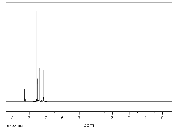
氢谱1HNMR
-
质谱MS
-
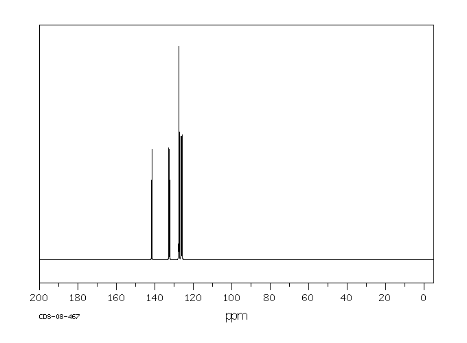
碳谱13CNMR
-
红外IR
-
拉曼Raman
-
峰位数据
-
峰位匹配
-
表征信息
同类化合物
(S)-溴烯醇内酯
(R)-3,3''-双([[1,1''-联苯]-4-基)-[1,1''-联萘]-2,2''-二醇
(3S,3aR)-2-(3-氯-4-氰基苯基)-3-环戊基-3,3a,4,5-四氢-2H-苯并[g]吲唑-7-羧酸
(3R,3’’R,4S,4’’S,11bS,11’’bS)-(+)-4,4’’-二叔丁基-4,4’’,5,5’’-四氢-3,3’’-联-3H-二萘酚[2,1-c:1’’,2’’-e]膦(S)-BINAPINE
(11bS)-2,6-双(3,5-二甲基苯基)-4-羟基-4-氧化物-萘并[2,1-d:1'',2''-f][1,3,2]二氧磷
(11bS)-2,6-双(3,5-二氯苯基)-4羟基-4-氧-二萘并[2,1-d:1'',2''-f][1,3,2]二氧磷杂七环
(11bR)-2,6-双[3,5-双(1,1-二甲基乙基)苯基]-4-羟基-4-氧化物-二萘并[2,1-d:1'',2''-f][1,3,2]二氧杂磷平
黄胺酸
马兜铃对酮
马休黄钠盐一水合物
马休黄
食品黄6号
食品红40铝盐色淀
飞龙掌血香豆醌
颜料黄101
颜料红70
颜料红63
颜料红53:3
颜料红5
颜料红48单钠盐
颜料红48:2
颜料红4
颜料红261
颜料红258
颜料红220
颜料红22
颜料红214
颜料红2
颜料红19
颜料红185
颜料红184
颜料红170
颜料红148
颜料红147
颜料红146
颜料红119
颜料红114
颜料红 9
颜料红 21
颜料橙7
颜料橙46
颜料橙38
颜料橙3
颜料橙22
颜料橙2
颜料橙17
颜料橙 5
颜料棕1
顺式-阿托伐醌-d5
雄甾烷-3,17-二酮

联系我们


关注我们

公众号

